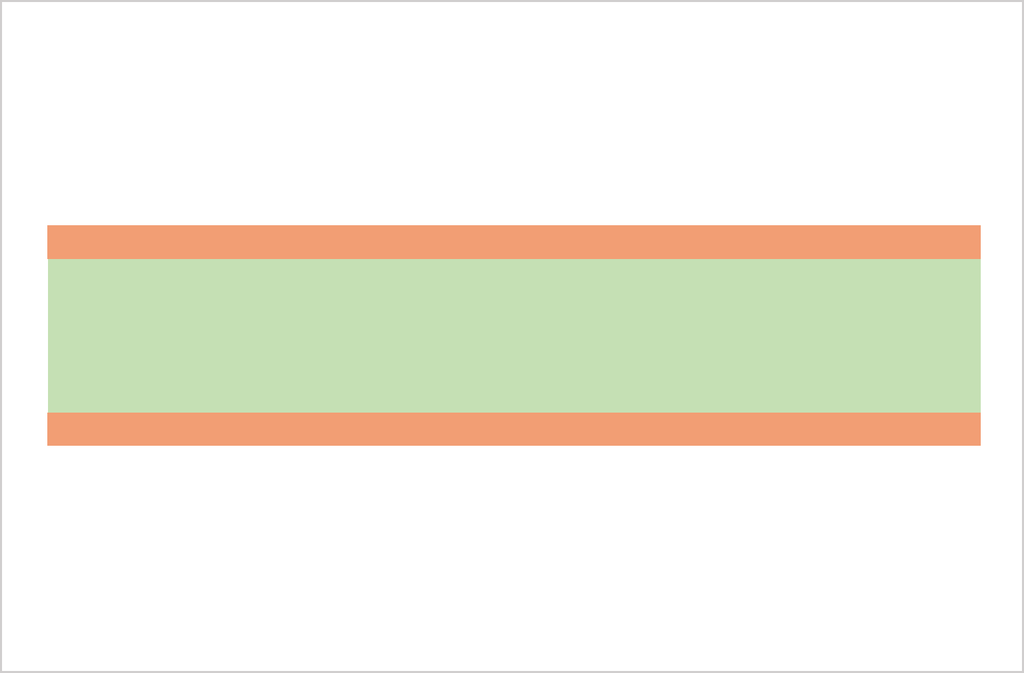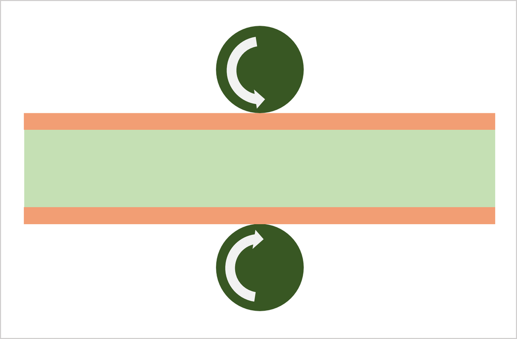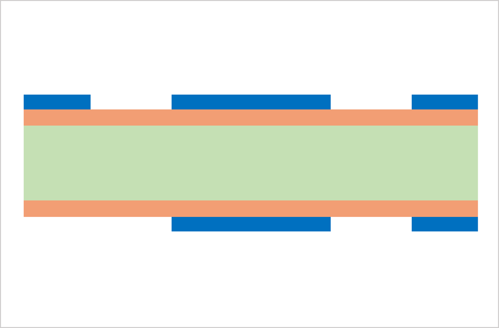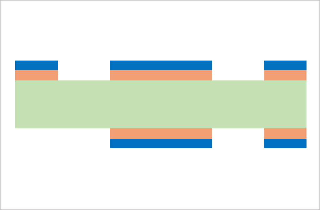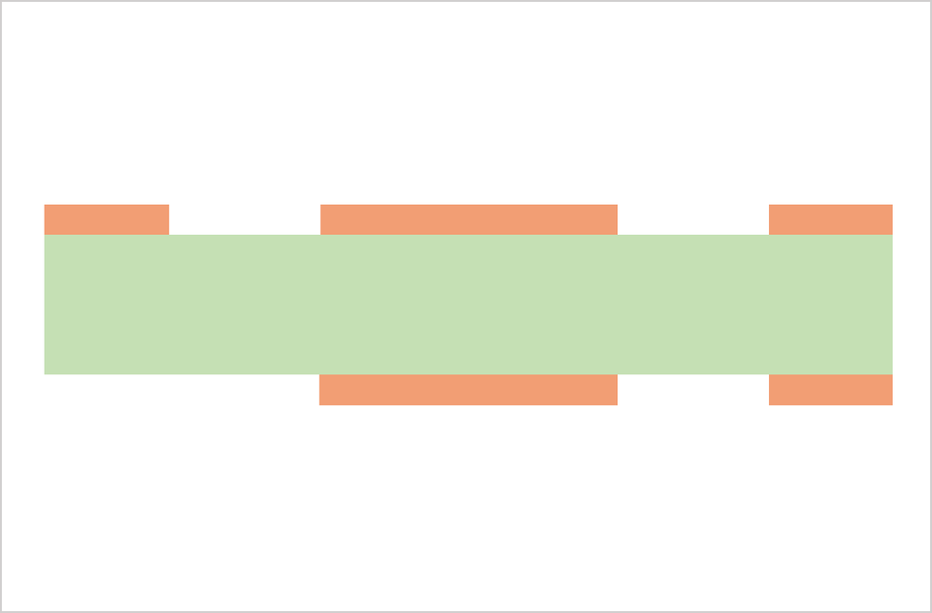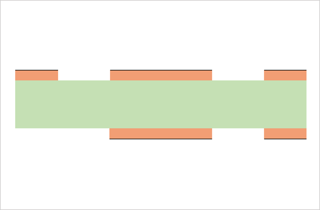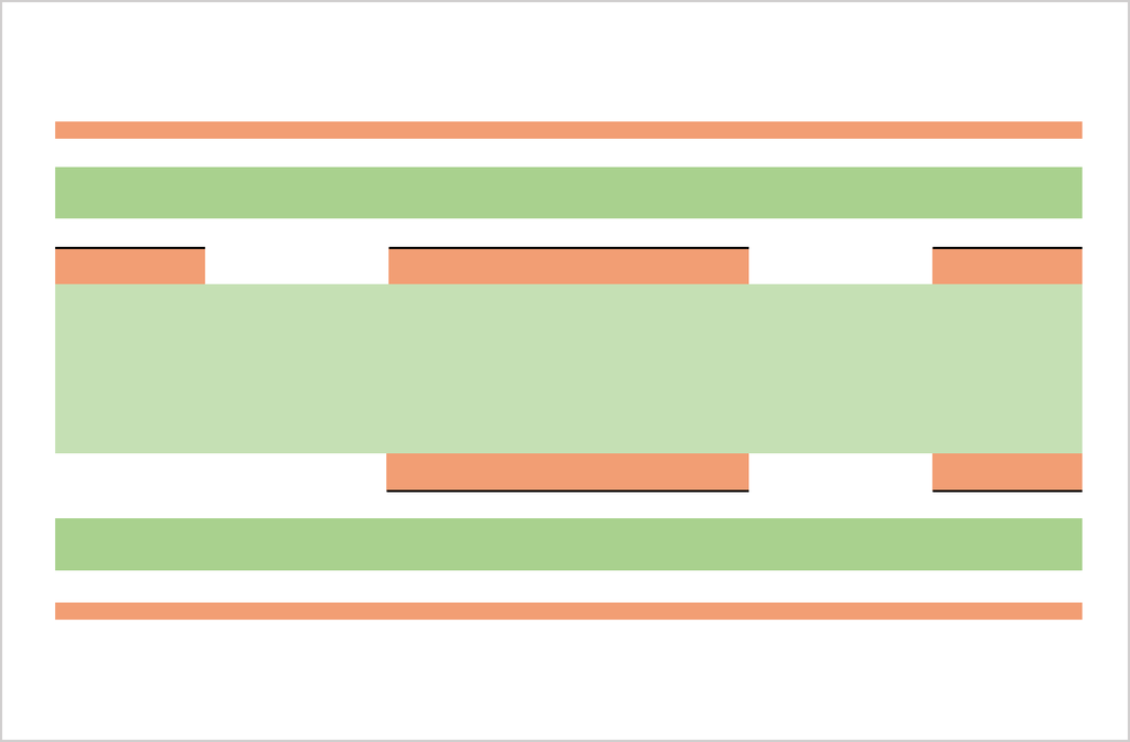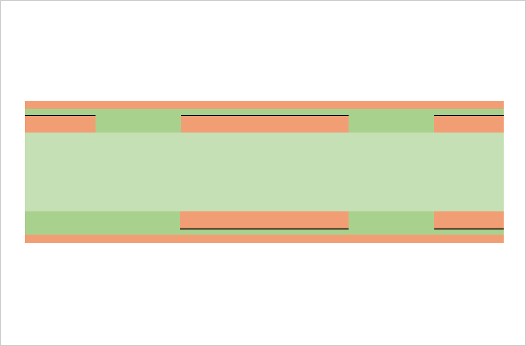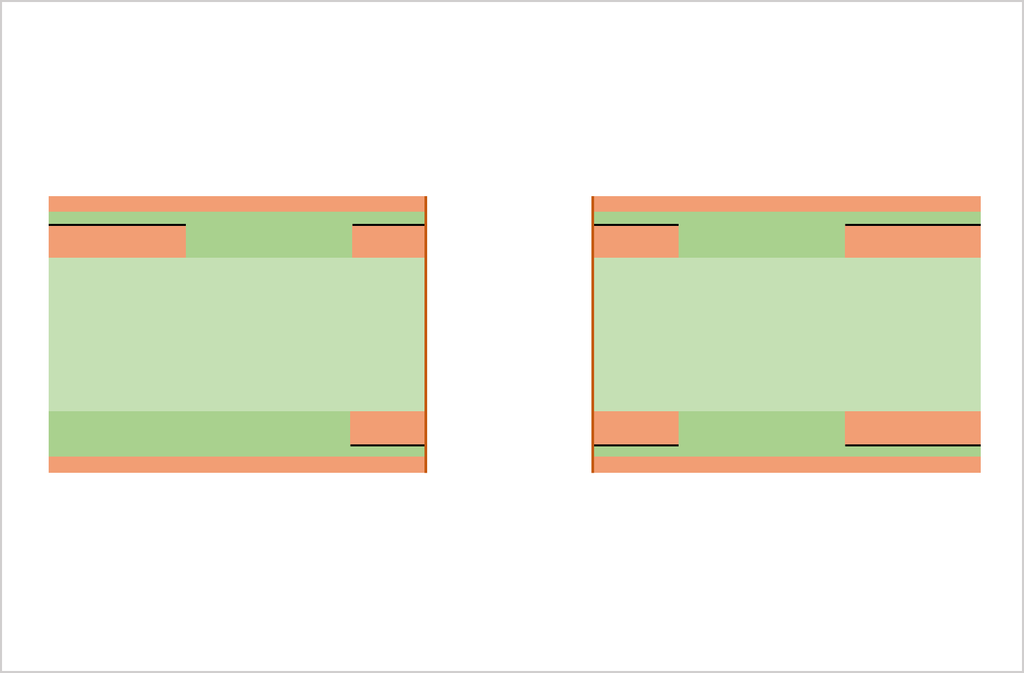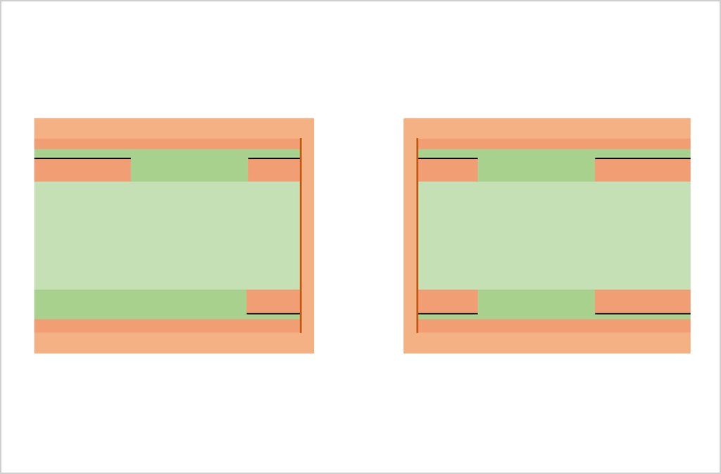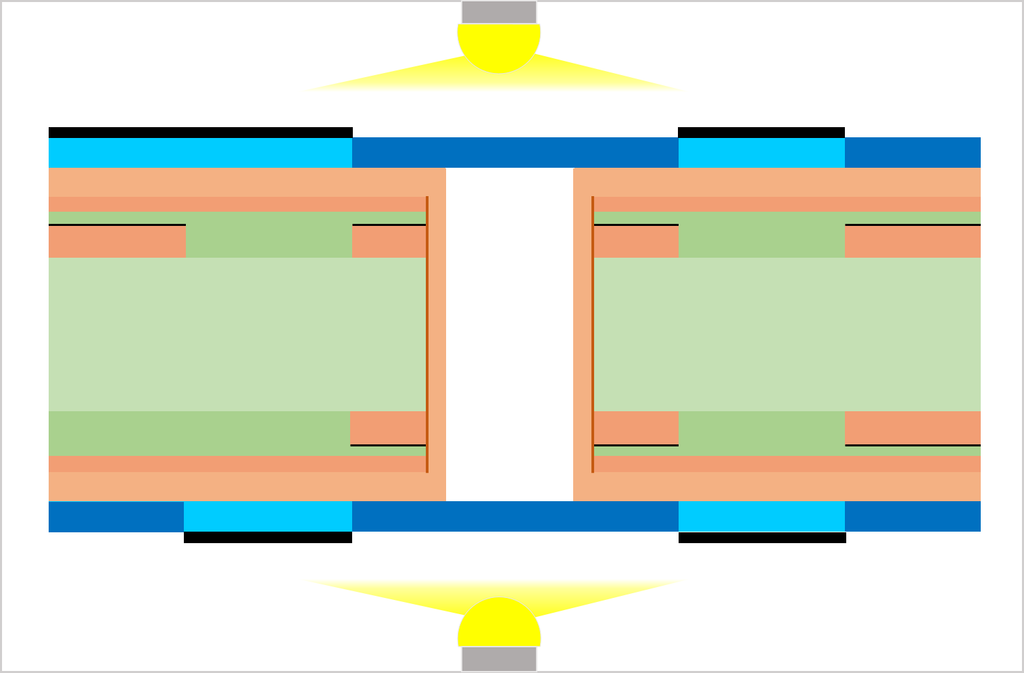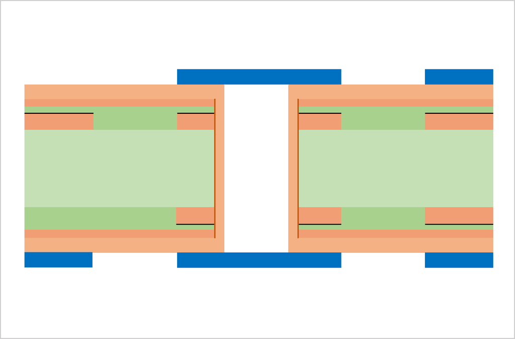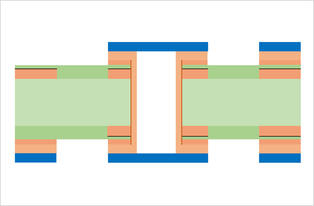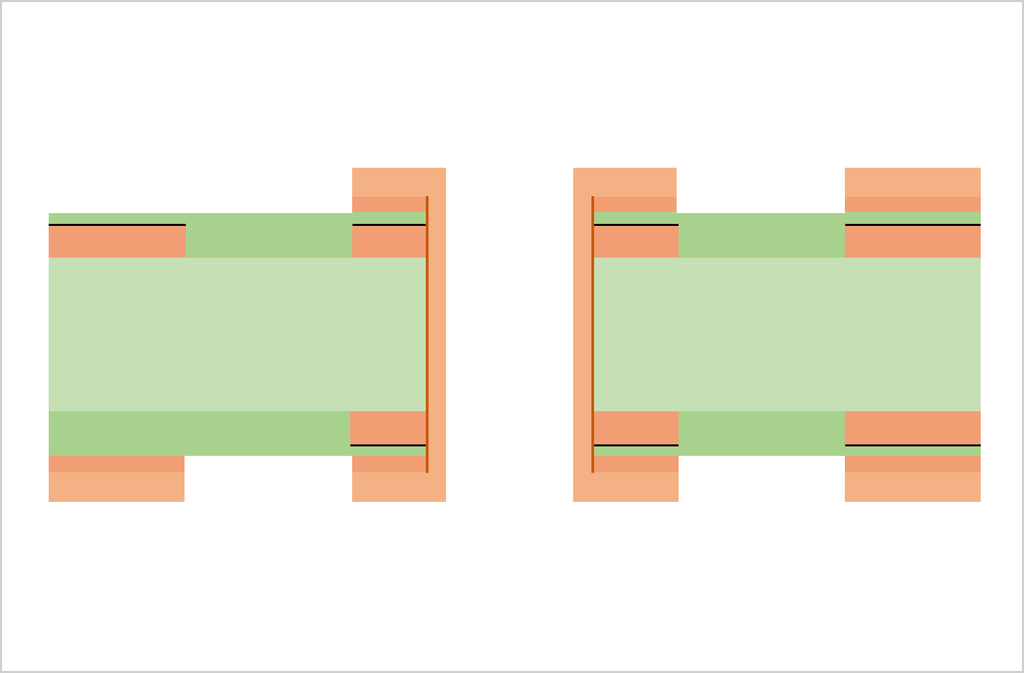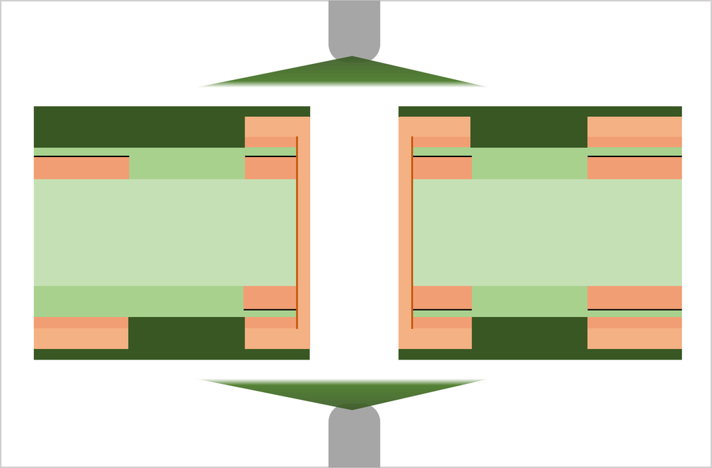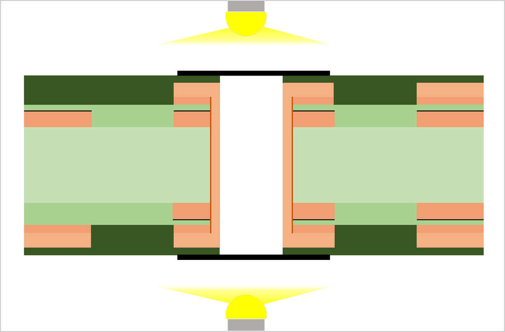
Substrate, cutting, PWB tooling-hole drilling
CCL (Copper Clad Laminate) is used as a substrate. Conduct board sizing and tooling-hole drilling. The tooling holes are used to align top-side and bottom-side circuits as well as inner and outer copper layers in a right position.