2025.12.23표면처리전시회정보
제27회 반도체・센서 패키징전 반도체 후공정 전문전 (ISP) 출전 안내
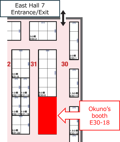
2026년 1월 21일(수)~23일(금)에 TOKYO BIG SIGHT서 개최되는 "제27회 반도체・센서 패키징전 반도체 후공정 전문전(ISP) "에 출전합니다. 사원 일동 모두 여러분의 방문을 진심으로 기다리고 있겠습니다.
- 일시
-
2026년 1월 21일(수)~23일(금)
- 개최 장소
-
도쿄 빅사이트, 동7홀, 【E30-18】
- 내용
-
Surface finishing technology to glass substrates
- Highly adhesive plating process on glass
- Acid copper plating additive for through-hole filling to glass core substrates
Plating technology for semiconductor wafer
- UBM formation for Al electrode on wafer
- Electroless plating equipment for wafer to make UBM
- Acid copper plating additives to semiconductor wafer
- Acid copper plating additive for Cu-Cu hybrid bonding
- Electroless plating process for insulated heat dissipation substrate (for power modules)
Plating technology for IC substrates
- Electroless copper plating process to solve Weak-Micro Via for high connection reliability
- Acid copper plating additive for high-current density, fine pattern via filling
- Acid copper plating additive for large diameter via filling
- Highly-reliable granular copper plating technology with high adhesion to molding materials
The latest surface finishing process
- New mist CVD equipment for next-generation power semiconductor : r-GeO2(under development)
- URL
- https://blog.naver.com/reed_japan/223336855920