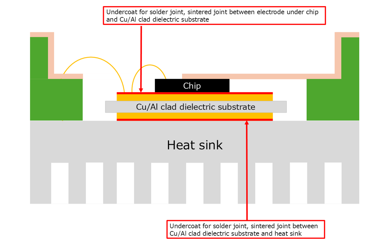
TOTAL
PROCESS
토탈 프로세스

Electroless plating process for Direct Copper Bonding (DCB) dielectric ceramic substrates

Power semiconductors, also known as power devices, are used to control and convert electrical power. They are widely used in power generation, bullet trains, trains, automobiles, and everyday household appliances like smartphones, computers, and refrigerators. Power semiconductors has been made with silicon (Si), which has a stable structure. However, power semiconductors made with silicon carbide (SiC) are now gaining attention due to their excellent heat resistance and long-term reliability. Additionally, research is progressing on sintering bonding using metal nanoparticles, such as copper and silver, as an alternative to solder bonding to achieve higher thermal conductivity and heat resistance. OKUNO offers a wide range of surface treatment chemicals for power semiconductor industries. We will introduce our product lineup that supports the manufacturing processes for Direct Copper Bonding (DCB) dielectric ceramic substrates.

 Electroless plating process for Direct Copper Bonding (DCB) dielectric ceramic substrates

  • CleaningProduct name ICP CLEAN T-2

    Remove dirt and resist residues from copper surface, improve surface wettability.

    Cleaning

  • Soft etching

    With sodium persulfate-sulfuric acid solutions or the likes, remove oxide films and create fine unevenness on the surface.

    Soft etching

  • Surface activation

    With sulfuric acid solutions or the likes, activate copper surface.

    Surface activation

  • Pre-dipping

    Pre-immerse in a hydrochloric acid dilution, which is an acidic component of the catalyzing solution. To prevent reducing the acid concentration in the catalyzing bath, proceed to the next step without water rinse.

    Pre-dipping

  • CatalyzingProduct name ICP ACCERA series

    Substitute the activated copper surface with metallic palladium.

    Catalyzing

  • Post-dippingProduct name ICP POSTDIP series

    Mask or remove Pd residues adsorbed outside the patterns to inhibit the spreading of electroless nickel plating

    Post-dipping

  • Electroless nickel platingProduct name ICP NICORON series

    Immerse into an electroless nickel plating solution containing nickel salts, reducing agents, and chelating agents. Nickel deposits by immersion reaction with zinc, and plating progresses through a self-catalytic reaction, forming a dense nickel film.

    Electroless nickel plating

  • Electroless palladium platingProduct name PALLATOP LP

    Obtain a palladium plating film with excellent heat resistance and barrier properties.

    Electroless palladium plating

  • Electroless gold platingProduct name NPG FLASH GOLD SR

    Obtain a gold plating film with excellent solder wettability, solder joint performance, gold wire bonding performance.

    Electroless gold plating