Featured
OKUNO's electroless copper plating process to solve Weak-Micro Via
OPC FLET PROCESS
In semiconductor package substrates (IC substrates), the demand for further micro-patterning and ultra-micro vias has increased due to the miniaturization, higher performance and increased functionality of electronic devices.
Via diameter in semiconductor package substrates has generally been around 80 µm; however, 50 µm vias have been introduced in recent years.
As via diameters continue to downsize, the connection areas of vias and inner copper layers will become significantly smaller. In this case, if conventional products are used, we will have adhesion problems of the connection reliability because we can’t ensure sufficient adhesion between the interface of inner copper layers and electroless copper plating.
To ensure high connection reliability in future semiconductor package substrates, we have developed a new electroless copper plating process, OPC FLET PROCESS.
Product features, specifications
When conventional electroless copper plating products are used on high-end PWBs for semiconductor package substrates, the connection reliability of vias and inner copper layers will decrease. This is because electroless copper plating films exist between the copper plating and the inner copper layers, and in addition, many nano-voids will also appear at the interface of the electroless copper plating films and the inner copper layers.
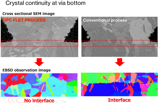
Our new electroless copper plating process, OPC FLET PROCESS, optimizes the catalyzing process resulting in thinner, higher purity electroless copper plating film. This allows for the crystal continuity of the plated copper films and the inner copper layers during the recrystallization of the copper electroplating films. In addition, the formation of nano-voids at the interface with the inner copper layer can be largely suppressed.
Furthermore, by reducing the thickness of the electroless copper plating, it is possible to reduce the amount of copper dissolved during the flash etching step, which can help to achieve ultra-micro patterning by SAP (Semi Additive Process).
This process contributes to solve the Weak-Micro Via problem (initial failures and aging failures) caused by the fracture between micro-vias and the inner copper layers.
OKUNO's electroless copper plating process to solve Weak-Micro Via
Our new electroless copper plating process, OPC FLET PROCESS, optimizes the catalyzing process resulting in thinner, higher purity electroless copper plating film. This allows for the crystal continuity of the plated copper films and the inner copper layers during the recrystallization of the copper electroplating films.