Electroless copper plating
For IC substrates in the next generation
- OKUNO's electroless copper plating process -
Smartphones are widely used not only for phone calls but also for enjoying music and movie, online shopping, cars, smart home appliances, robots.
The technology about smartphones, tablet computers and other telecommunication devices are rapidly progressing, and the maximum transmission speed in telecommunications has increased about 1,000,000 times in 30 years. Furthermore, next-generation communication system requires extremely advanced performance also for the semiconductors that will be used in high-speed and high-class servers and computers.
OKUNO's new electroless copper plating process, "OPC FLET PROCESS", received the award of the 26th Symposium on Microjoining and Assembly Technology in Electronics (Mate 2020), which was mainly organized by Manufacturing Science & Technology in Electronics in SMART PROCESSING SOCIETY FOR MATERIALS, ENVIRONMENT & ENERGY.
OKUNO are committed to challenge any of materials such as ultra-low profile copper foils, newly developed dielectric materials to support the latest electronics industry.
Please feel free to contact us from the web inquiry form making prototypes to mass-production.

Miniaturization technology for PWB
As electronic devices become lighter, thinner, smaller, high density semiconductors are more strongly demanded for IC substrates.
For that reason, the size of circuit patterns and via-holes becomes smaller and smaller; additionally, the thickness of inner copper foils is remarkably decreasing.
Around via-holes, three types of copper: an inner copper layer (mainly made by copper electroplating), electroless copper plating and copper electroplating films exist.
Until now, if conventional products are used for PWBs in recent years, we have adhesion problems of connection reliability because sufficient adhesion can't be ensured between the interface of inner copper layer and electroless copper plating.
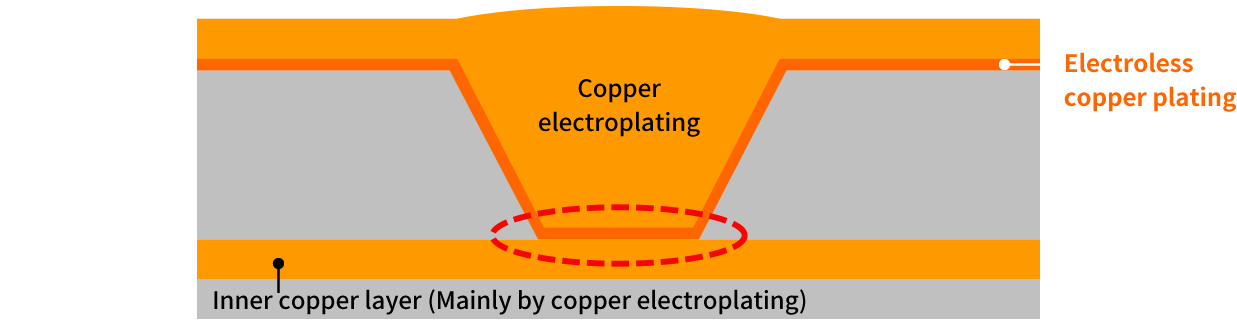

Decrease connection reliability because sufficient adhesion can't be ensured around via-bottom
Enables ultra-micro circuit pattern formation below L/S=5/5μm
OKUNO's electroless copper plating process
OPC FLET PROCESS
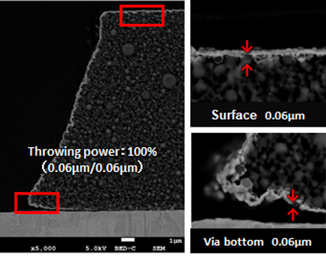
OKUNO has newly developed an electroless copper plating process, "OPC FLET PROCESS". OPC FLET PROCESS enables to form copper seed layers with high covering performance and great electric conductivity by small thickness. Also, high adhesion can come available at the bottom of via-holes even on low roughness substrates.
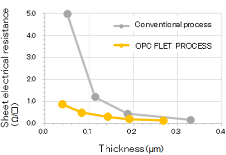
By reducing the thickness of electroless copper plating, we succeed to minimize the damage and loss of circuit patterns in seed layer etching steps.
This technology enables to drawing ultra-micro circuit patterns below Line/Space=5/5μm.
Ensure high covering performance by small thickness in via-holes
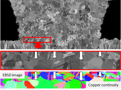
■OPC FLET PROCESS
Increase electric conductivity with small thickness
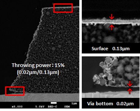
■Conventional process
Ensure high peel strength even on low profile substrates
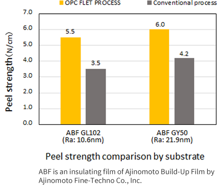
Ensure high connection reliability between inner copper layer and plated copper films
OKUNO has newly developed an electroless copper plating process, "OPC FLET PROCESS" that enables to achieve crystal continuity at the interface of inner copper layers and electroless copper plating.
To expand your possibilities into new IC substrates, please contact us from the web inquiry form. Achieve the highest connection reliability for advanced telecommunication era together.
■OPC FLET PROCESS
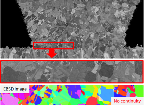
■Conventional process
■For IC substrates in the next generation OKUNO's electroless copper plating process OPC FLET COPPER
For bright future, we continue to develop innovative products and services and to provide advanced technology for any of new materials. If you need more information, please contact from web inquiry form.