Featured
Additive for acid copper plating with high via-filling performance to large diameter holes for fine patterns
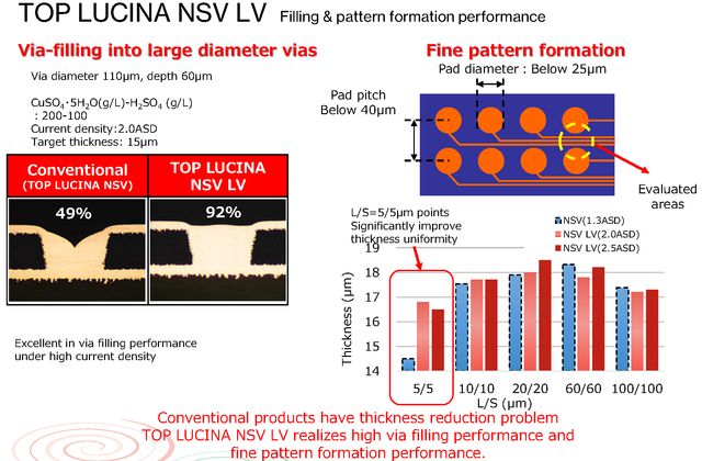
TOP LUCINA NSV LV
The pace of development of electronic devices, such as smart phones, continues to amaze. As electronic devices become more sophisticated and compact, high-density patterning, thinner packages and narrow-pitch technology for PWBs are in high demand.
Semiconductor packaging substrates are manufactured by the semi-additive process, and each layer is interconnected by via-fill plating. However, when conventional via-fill plating additives are used for high-density PCBs, there are problems with thickness uniformity and via-fill performance in fine patterning.
As circuits become finer, it becomes increasingly difficult to achieve both thickness uniformity and good via fill performance. To address this issue, we've developed a new additive for electrolytic copper (copper sulfate) plating.
Product features, specifications
In the development of TOP LUCINA NSV LV, we have optimized the molecular structure of the inhibitors to achieve both further pattern plating film thickness uniformity and excellent via filling performance.
As a result, it is now possible to achieve both large-diameter via filling plating at higher current density and film thickness uniformity in fine patterns than with conventional products.
This product achieves via filling by filling the inside of vias with copper plating, which has been difficult to achieve with conventional products, and can be used for a wide range of applications from build-up layers to core layers, contributing to improved productivity and reliability of PWBs.
Additive for acid copper plating with high via-filling performance to large diameter holes for fine patterns
TOP LUCINA NSV LV achieves via filling by filling the inside of vias with copper plating, which has been difficult to achieve with conventional products, and can be used for a wide range of applications from build-up layers to core layers, contributing to improved productivity and reliability of PWBs.