Total process

OKUNO's process for the manufacture of semiconductor package substrates

OKUNO provides a wide variety of plating chemicals as total process in order to support the rapid developments of IC substrates, plastic semiconductor substrates and plastic interposers for CPU (Central Processing Unit), GPU (Graphics Processing Unit) and other semiconductor devices.
We explain the manufacturing steps about the semiconductor substrates by semi additive process (SAP) including our products.

OKUNO's process for the manufacture of semiconductor package substrates

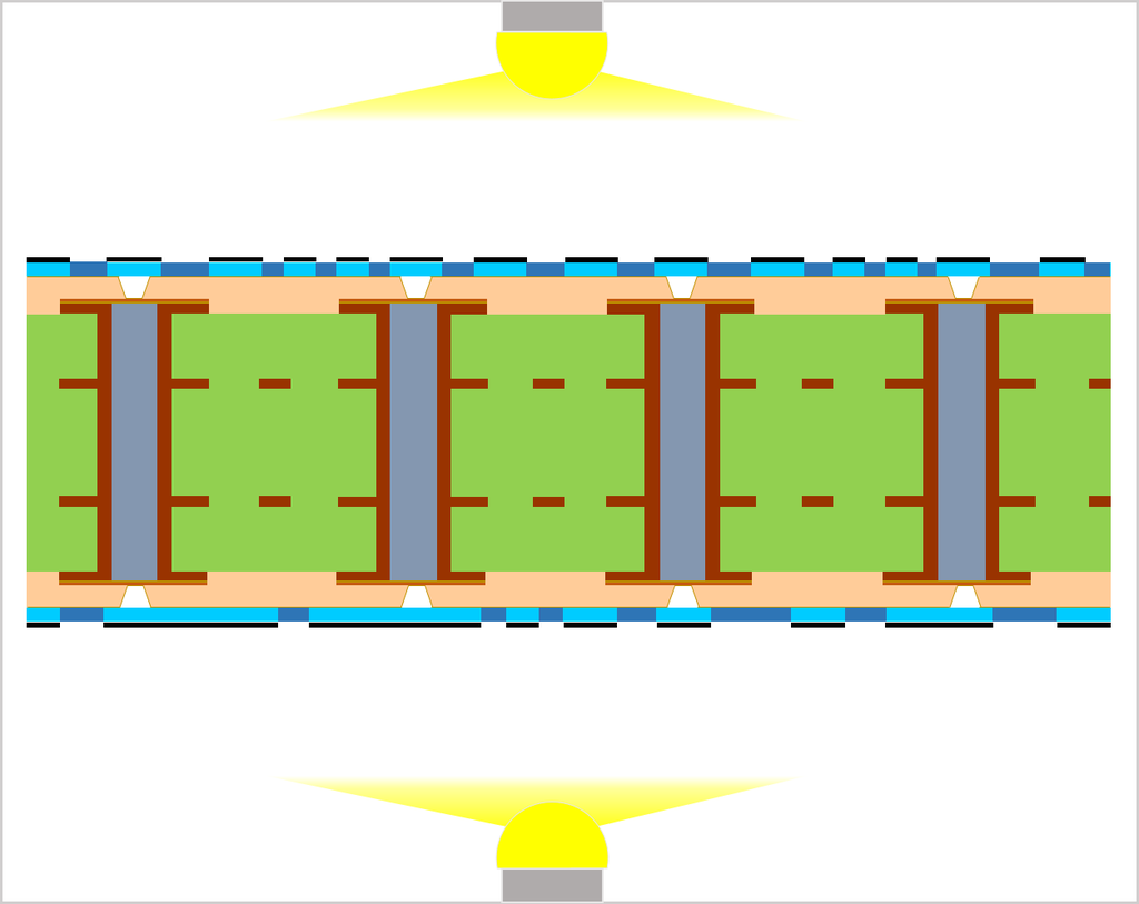
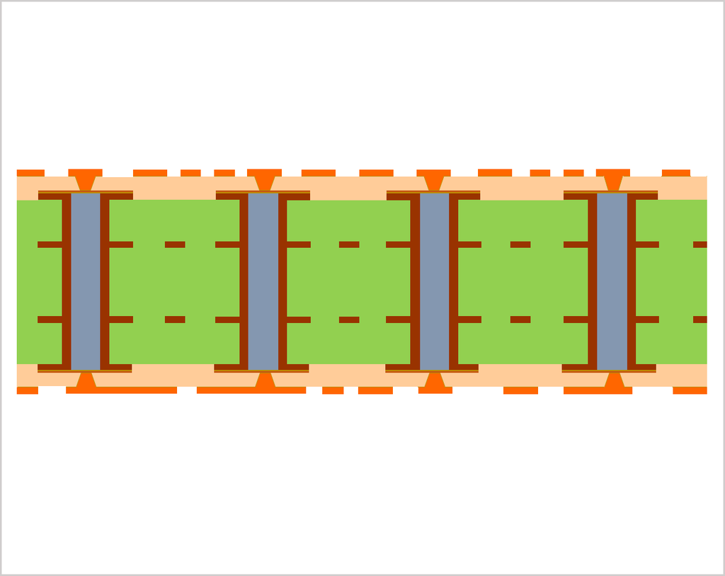
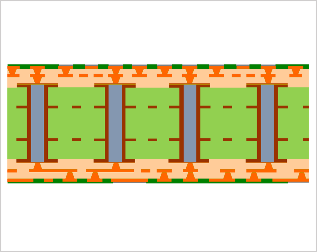
  • Plug-in into through holes

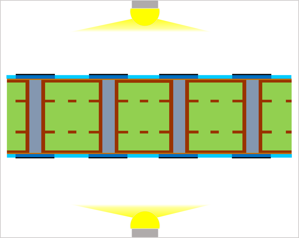
    Multi-layer (ex. 4 or 6 layer) printed wiring boards are used as the core for semiconductor substrates. Here, we start detailed explanation about the manufacturing process after the copper electroplating step into through holes. You can learn more information before the copper electroplating into through holes by our website, "Contribute PWB fabrication by OKUNO’s total solutions".
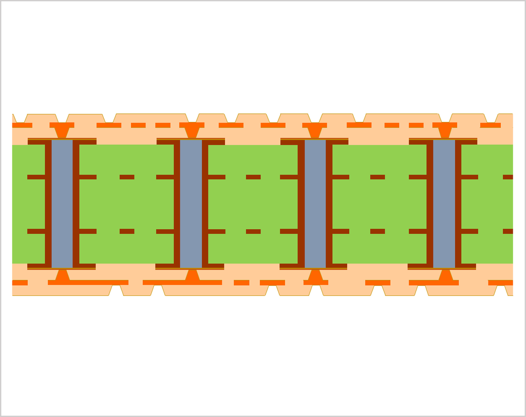
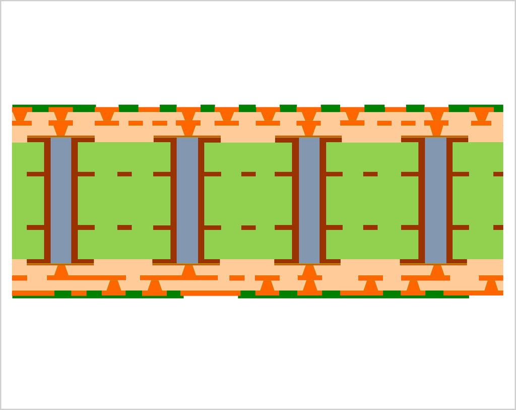
    Roughen copper electroplating surface by annealing or other methods.
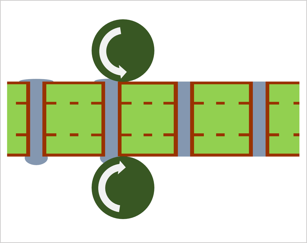
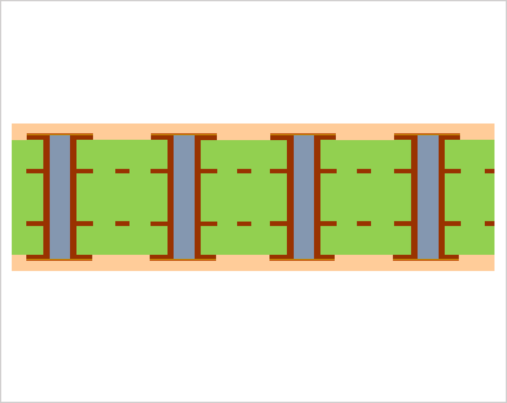
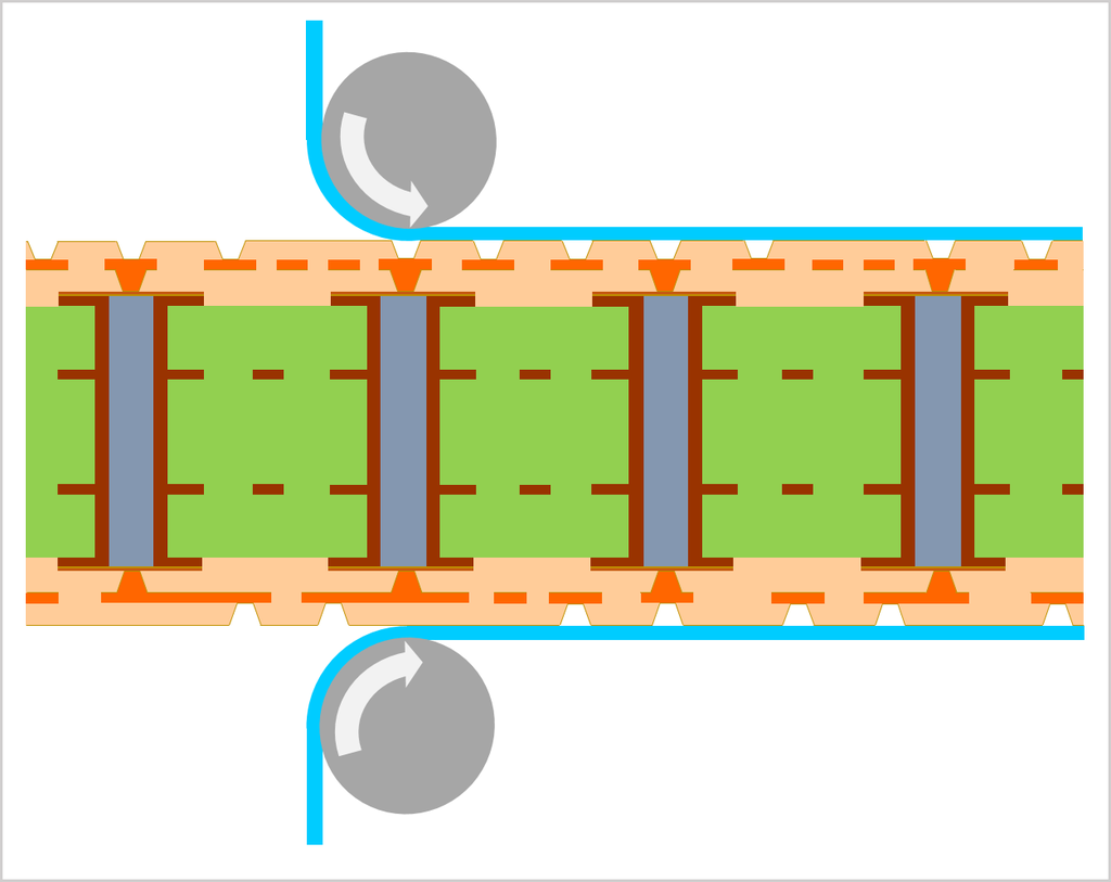
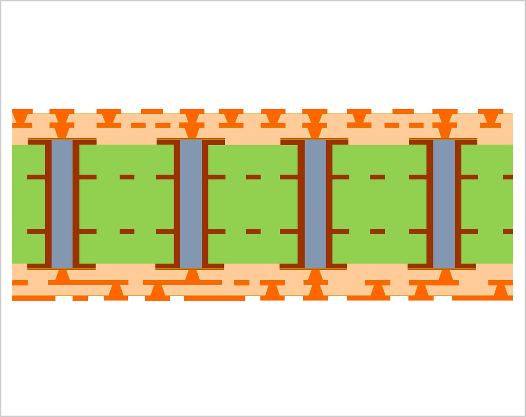
    Fill each through holes with thermosetting inks (Hole Plugging Process).
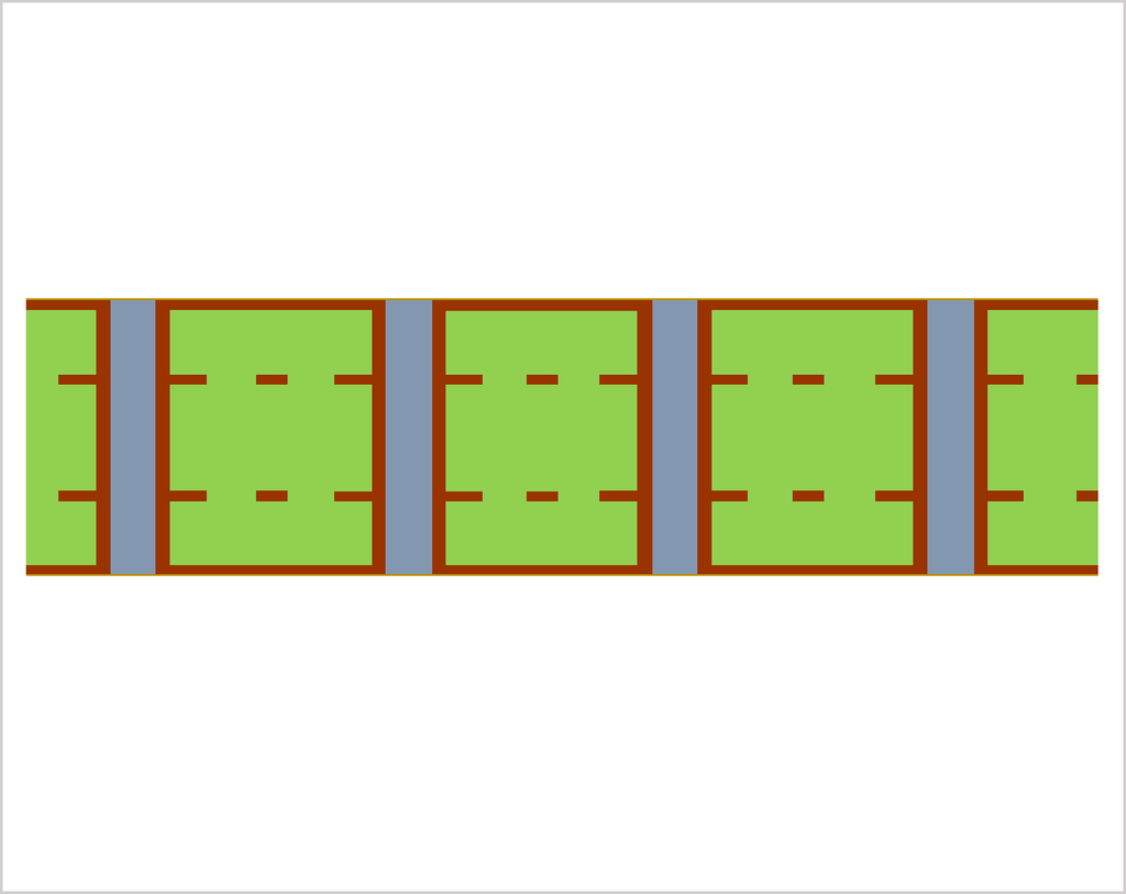
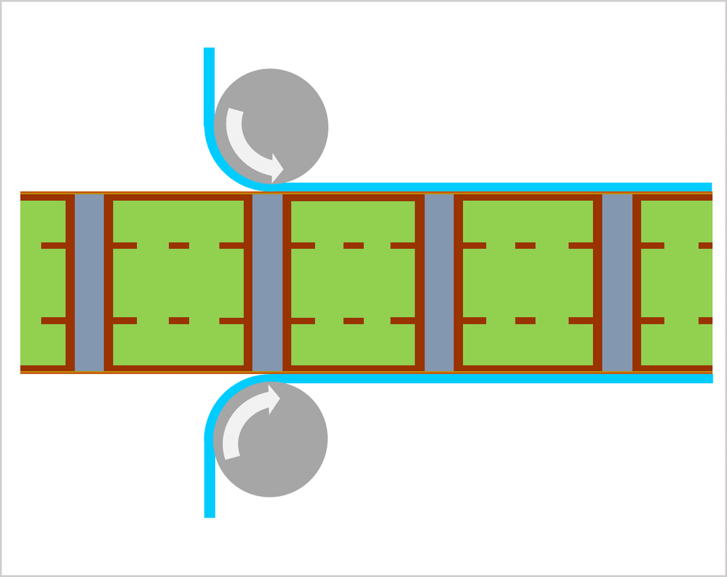
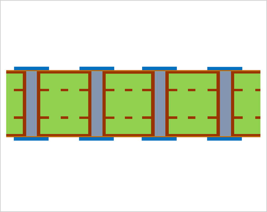
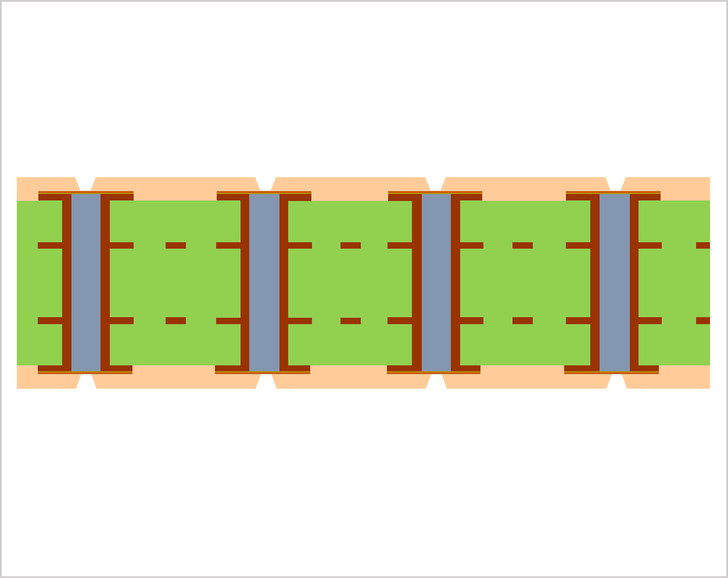
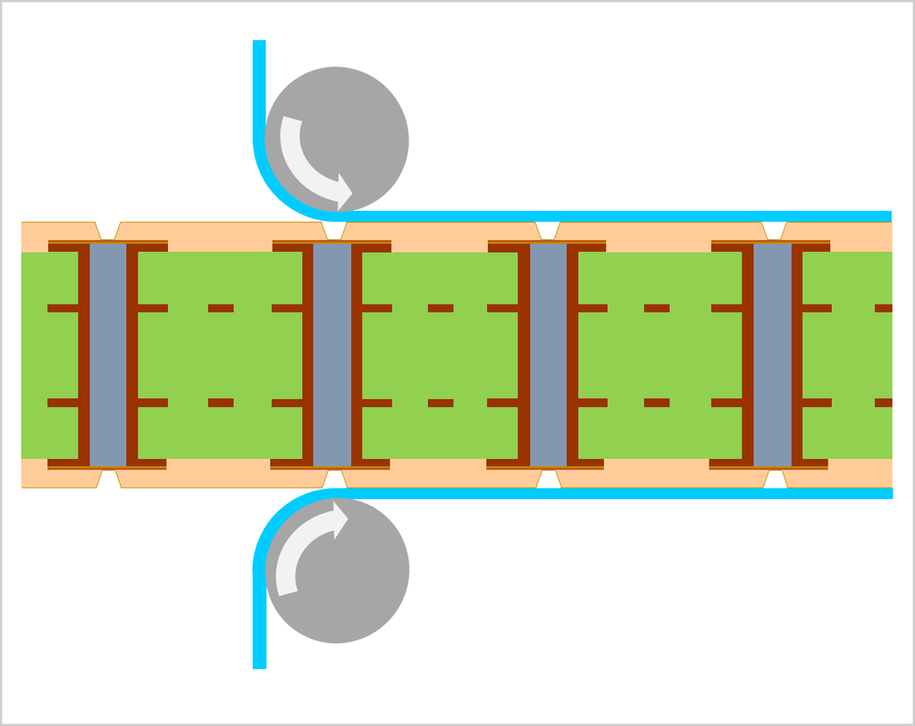
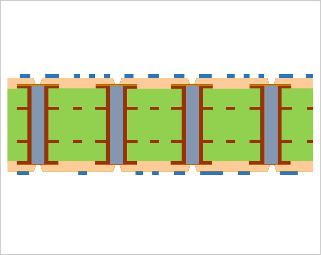
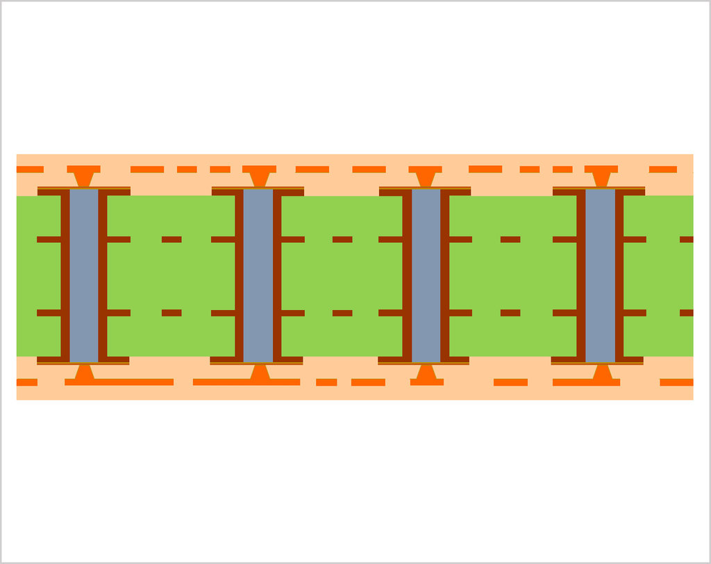
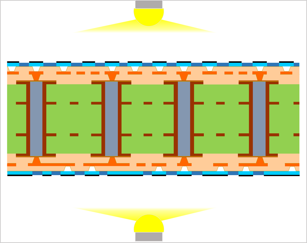
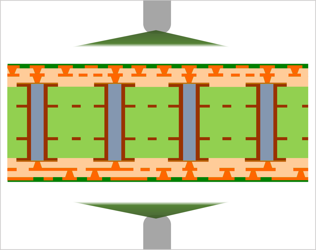
    Dry the inks, and remove ink residues at the both sides of the printed wiring board.
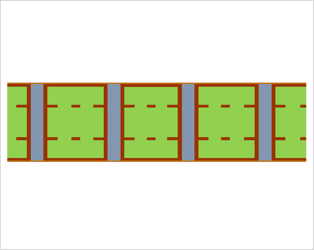
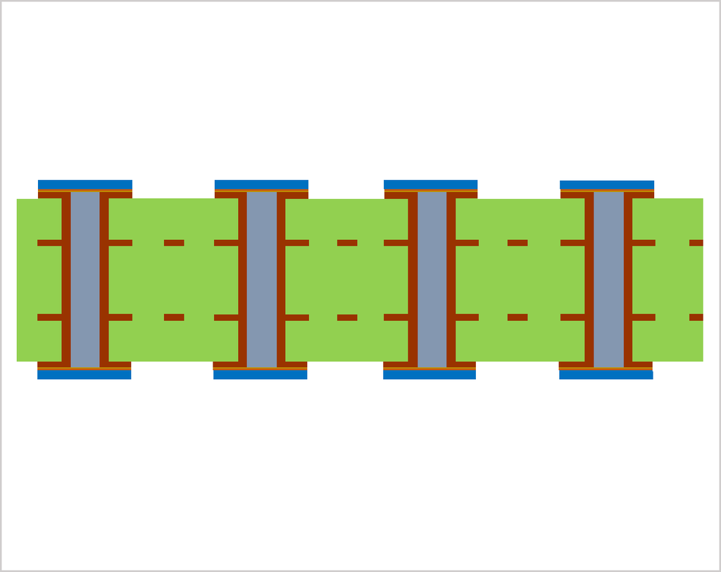
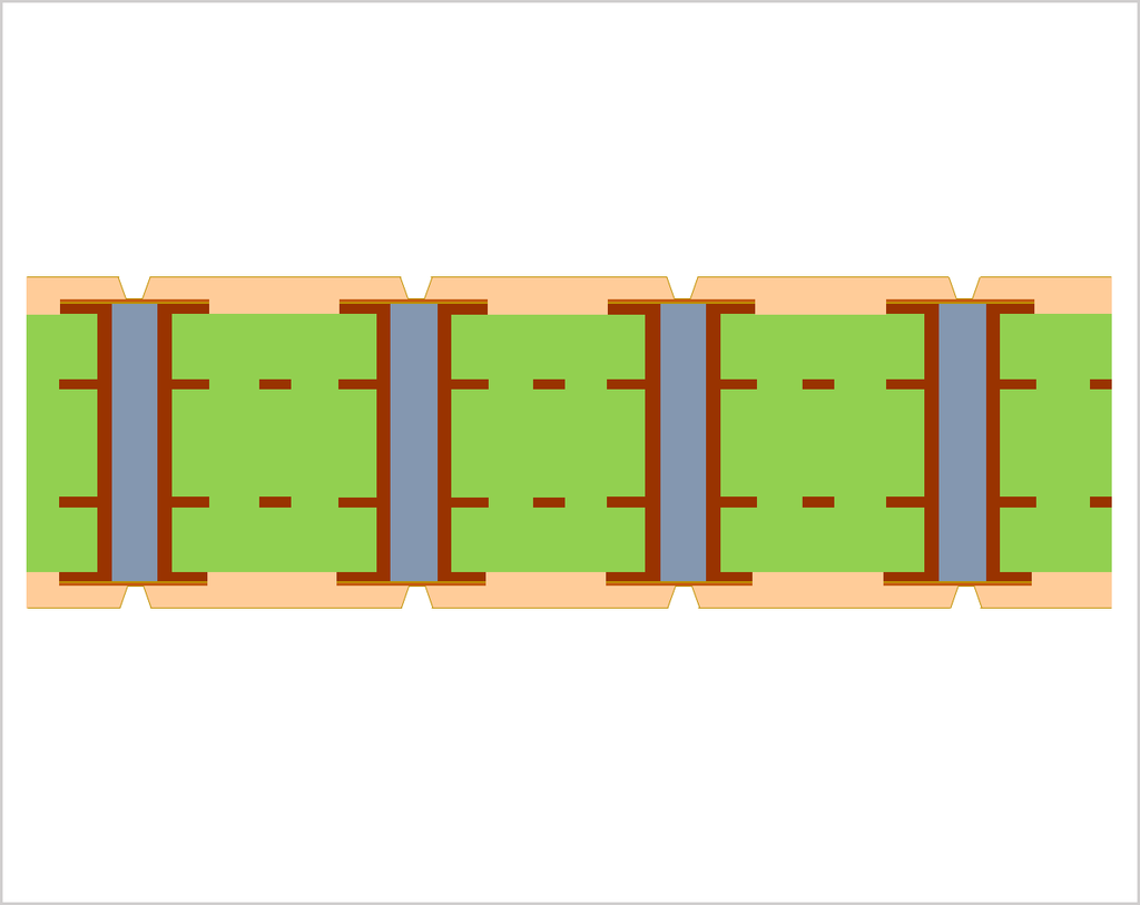
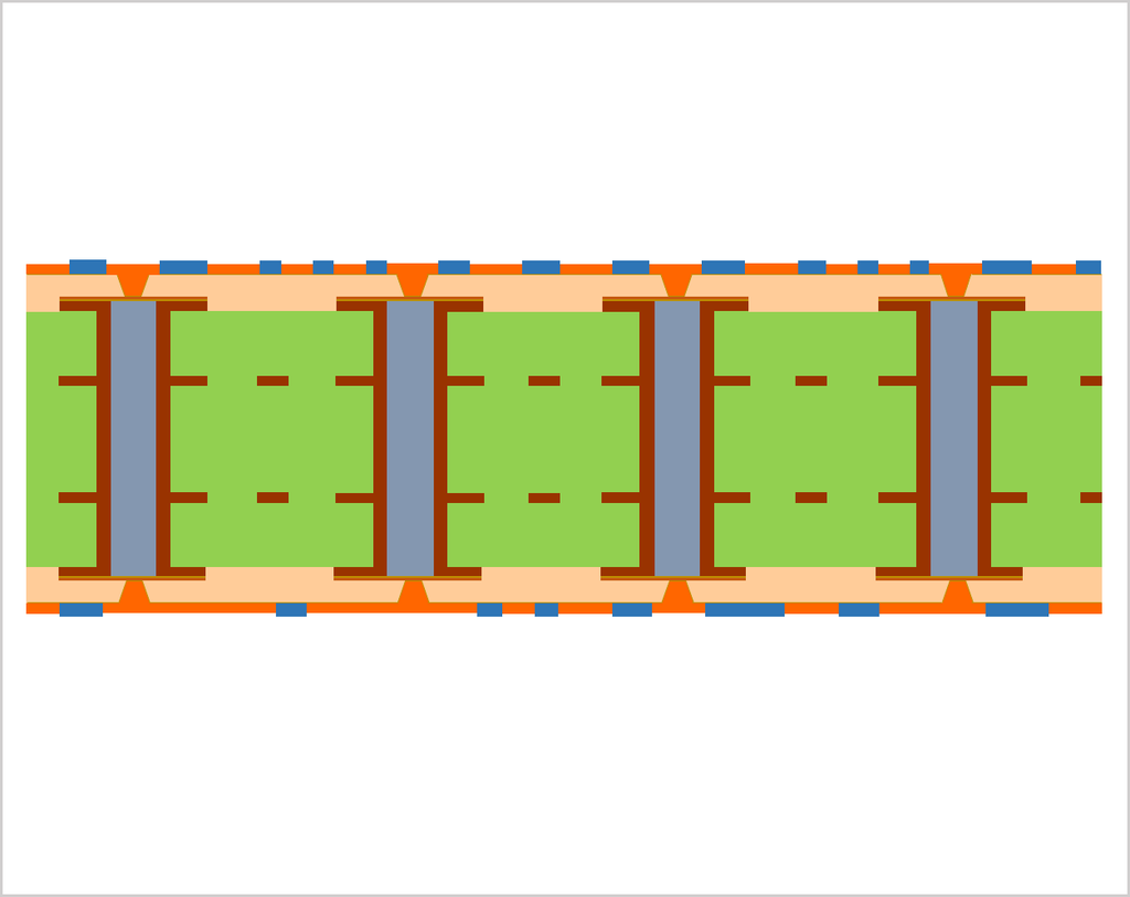
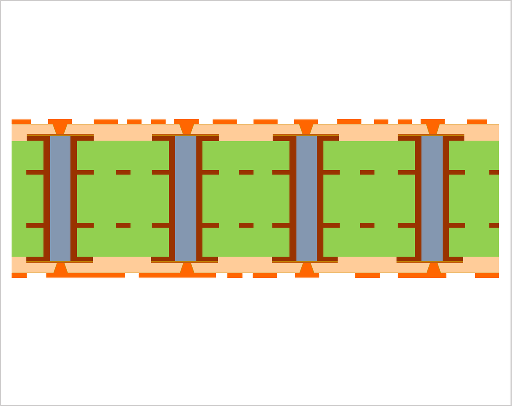
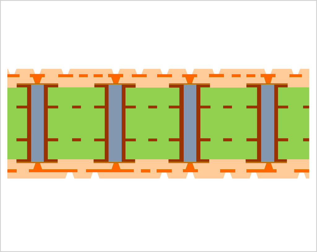
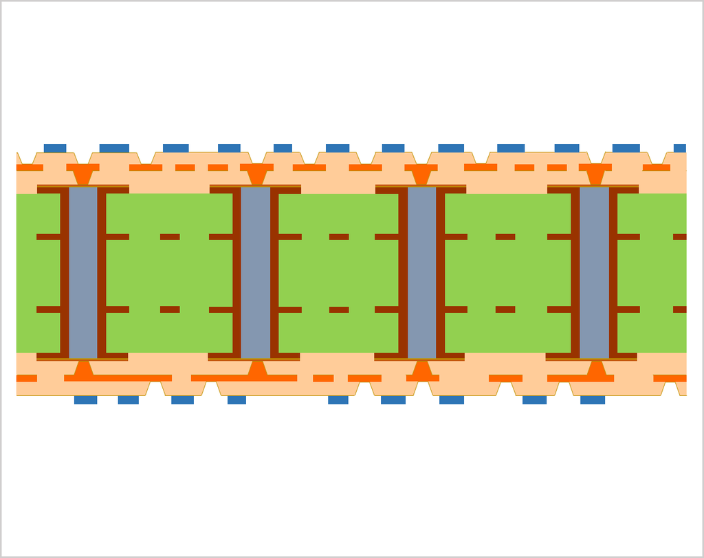
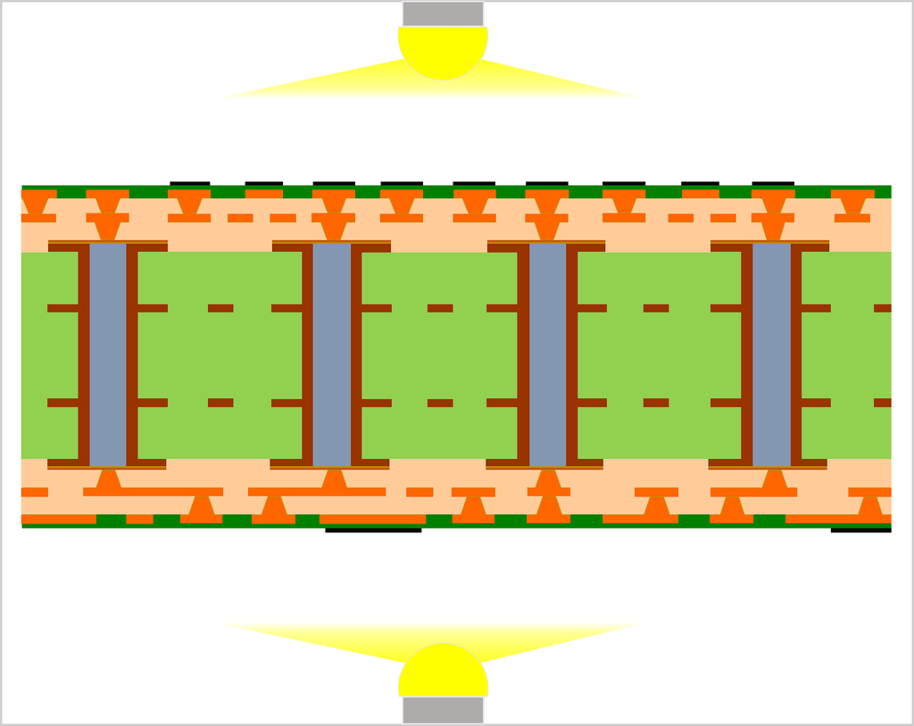
    Completely cure the inks.
    If through holes are fully filled by the copper electroplating, the steps from plug-in to electroless copper plating can be omitted.
    Also, filling by the electroplating can increase thermal conductivity, so some companies have made the filling by the electroplating practical.
    For full filling into through holes by the electroplating, we have TOP LUCINA LTF and related products.

    plug-in into through holes

  • De-smear and electroless copper platingProduct name OPC-1000 PROCESS DS, OPC PROCESS, OPC H-TEC PROCESS

    Remove resin debris from the copper plating films on the PWB surface.
    Roughen ink-filled area, and conduct catalyzing and electroless plating.

    de-smear and electroless copper plating

  • Copper electroplatingProduct name TOP LUCINA series

    Conduct copper electroplating on the PWB surface.

    copper electroplating

  • DFR lamination

    Conduct pre-treatment(ex: scrubbing)on the PWB surface.
    Laminate dry film resist (DFR) on the copper plating films.

    dfr_lamination

  • DFR exposure

    Apply masks (films, metals or glass) partly on DFR and expose light onto the whole surface.

    dfr_exposure

  • DFR development

    Dissolve the mask-applied (unexposed) areas with sodium carbonate solution.
    The masks remaining on the copper plating films are used as a resist for a next etching step.

    dfr_development

  • Etching

    Etch the spaces among patterns with copper (II) chloride solution or an etching solution, and form circuit patterns.

    etching

  • DFR strippingProduct name OPC PERSORRY series, BUBBRAT R-2

    Strip DFR with an alkaline solution.
    Stripping bathes foam by using, so anti-foaming agents are generally used.
    Remove dry film resists.
    Etch the surface of copper plating films to ensure adhesion of the copper and insulating layers.

    dfr_stripping

  • Insulating layer lamination (Dielectric layer lamination)

    Laminate an insulation resin on the PWB surface to fabricate a build-up layer.
    Film-type insulation resin can be also used, and film-type resin are applied in a vacuum laminating machine.

    dielectric_layer_lamination

  • Laser drilling

    Conduct laser drilling, form via-holes.

    laser_drilling

  • De-smear and electroless copper platingProduct name OPC FLET PROCESS and related products

    Remove resin debris from the copper plating films on the PWB surface.
    Roughen ink-filled area, and conduct catalyzing and electroless plating.

    de-smear and electroless copper platin

  • DFR lamination

    Laminate dry film resist (DFR) on the copper plating films.

    dfr_lamination

  • DFR exposure

    Apply masks (films, metals or glass) partly on DFR and expose light onto the whole surface.
    In subtractive process, circuit patterns are exposed.
    In semi additive process, space areas between circuit patterns are exposed.
    Currently, LDI (Laser Direct Imaging), which doesn’t require mask application, is increasing.

    dfr_exposure

  • DFR development

    Dissolve the mask-applied (unexposed) areas with sodium carbonate solution.
    The masks remaining on the copper plating films are used as a resist for a next etching step.

    dfr_development

  • Pattern platingProduct name TOP LUCINA series

    Conduct the pattern plating that means the plating into via-holes and the circuit patterns at the same time.
    Via-holes can be filled by conformal plating or full filling plating.
    Now, Via on Via (Stacked vias) have prevails to achieve high density interconnection and small pitch mounting, so full-filling is applied to via-holes in many cases.
    Plating additives for copper electroplating (acid copper plating) requires macro-throwing power regardless of pattern density or pattern-size.
    Furthermore, high class via-filling performance is quite important.

    pattern_plating

  • DFR strippingProduct name OPC PERSORRY series, BUBBRAT R-2

    With an alkaline solution, remove unnecessary dry film resists.
    Different from the stripping of dry film resists in general subtractive process, high stripping power is especially in semi additive process because dry film resists are be surrounded by the copper plating films between fine patterns.
    Stripping bathes foam by using, so anti-foaming agents are generally used.

    dfr_stripping

  • Flash (quick) etching, surface roughening, and palladium residue removalProducy name OPC PALLADELETE S and related products

    Conduct flash (quick) etching to all of the surface areas to remove electroless copper plating films.
    In some cases, palladium, which is used as the catalysts for electroless copper plating, is removed after the flash etching to ensure high-level insulation property.
    Next, roughen the circuit surface by etching or other methods.

    flash_etching, surface_roughening, palladium_residue_removal

  • Insulating layer lamination (Dielectric layer lamination)

    Laminate an insulation resin on the PWB surface to fabricate a build-up layer.

    insulating_layer_lamination

  • Laser drilling

    Conduct laser drilling, form via-holes.

    laser_drilling

  • De-smear and electroless copper platingProduct name OPC FLET PROCESS and related products

    Remove resin debris from the copper plating films on the PWB surface.
    Roughen ink-filled area, and conduct catalyzing and electroless plating.

    de-smear and electroless copper platin

  • DFR lamination

    Laminate dry film resist (DFR) on the copper plating films.

    dfr_lamination

  • DFR exposure

    Apply masks (films, metals or glass) partly on DFR and expose light onto the whole surface.

    dfr_exposure

  • DFR development

    Dissolve the mask-applied (unexposed) areas with sodium carbonate solution.

    dfr_development

  • Pattern platingProduct name TOP LUCINA series

    Conduct the pattern plating that means the plating into via-holes and the circuit patterns at the same time.

    pattern_plating

  • DFR strippingProduct name OPC PERSORRY series, BUBBRAT R-2

    With an alkaline solution, remove unnecessary dry film resists.

    dfr_stripping

  • Flash (quick) etching, surface roughening, and palladium residue removalProducy name OPC PALLADELETE S and related products

    Conduct flash (quick) etching to all of the surface areas to remove electroless copper plating films. Remove palladium to ensure high-level insulation property and avoid the deposition between the patterns in electroless Ni/Au or other steps.

    flash_etching, surface_roughening, palladium_residue_removal

  • Solder resist application

    Apply PSR (Photo Solder Resist) on the through hole by screen printing or static printing. Film-type solder resist can be also used.
    Film-type solder resist is applied in a vacuum laminating machine.

    solder_resist_application

  • Solder resist exposure

    After pre-curing, apply masks around the through hole, and expose light onto the whole surface.

    solder_resist_exposure

  • Solder resist development

    Dissolve the solder-resist applied (unexposed) areas with an alkaline solution. Conduct post-curing.

    solder_resist_development

  • Final surface treatmentProduct name TOP ICP PROCESS, SUBSTAR SN series

    Electroless nickel/(palladium)/gold plating, electroless tin plating, solder leveling treatment (solder melting plating) are conducted for surface mounting. Before the electroless nickel plating, cleaning, catalyzing and post-dipping steps are necessary.

    OKUNO's TECHNOLOGY:「ELECTROLESS COPPER PLATING PROCESS FOR IC SUBSTRATES

    final_surface_treatment